Quartz crystal thin film sensors are routinely employed in the manufacture of thin film electronic devices such as OLED displays, CIGS solar cells and also ALD / CVD processes. While known for their ability to detect films as thin as one Angstrom and, when properly optimized, reliable enough to insure process repeatability, crystal derived thickness readings are often taken as indisputable measurements by process engineers. Unfortunately, this blind faith can have major negative consequences in the manufacture of sophisticated thin film products.

In a typical deposition run, the user programs the crystal controller with the density of the film being monitored, the acoustic impedance value (applicable only to thick films) and the tooling factor, a geometrical correlation of the deposition source to crystal and source to substrate distances. The primary assumption made is that the film density is known, and that it is not dependent on deposition conditions. For a given process configuration, the film density can be calculated exactly by comparing the crystal thickness with a secondary measurement obtained from profilometry, for example. If not, a significant error can be introduced to the film thickness calculation.
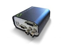
The Eon-ID™ is a new film thickness controller that
packages an ultra-high resolution deposition control system into a compact,
rack-mountable enclosure.
Featuring integrated display, intuitive GUI, and durable
architecture, Eon-ID™ offers an all-inclusive design that adapts easily to a
variety of settings – ranging from industrial to laboratory to clean room to
research environments. Eon-ID™ integrates well into existing rack thin film
systems.
Employing a unique temperature compensation system to monitor the
temperature of the Phoenix™ quartz crystal sensor, Eon-ID™ is the only
comprehensive solution of its kind that is capable of real-time temperature
measurement and source control.
Features include:

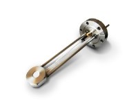
You've known the water-cooled sensor head holders, so it's time to discover the heated versions and why those high temperatures - sometimes up 500°C are so valuable for certain advanced processes.

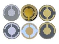
For years customer's around the world have ordered our AT-cut xtronix Quality Quartz Crystals. While these are ideal for the traditional markets they serve, technology evolves and new crystal products are now available.

Supporting our new crystal offering, the imporance of an advanced purpose-designed electronics is not to be underestimated. We now offer three monitors / controllers to meet various customer needs.
Temperature Measurement & Control of Quartz Crystal Microbalances... why you should insist on it!
The greatest source of error to film thickness measurement arises from factors not accounted for in a typical deposition. Although the quartz crystal resonance frequency has been shown to be sensitive to mass deposition, it also is sensitive to temperature, stress in the growing film, and adhesion of the film to quartz, among other factors. The temperature dependence is so great that quartz has been used as a thermometer.
Unless process engineers and product designers account for the quartz crystal temperature effects and other unique variables, they will be unable to guarantee that run to run reproducibility will be possible for their thin film product. Worse, successful products developed under strict protocols in a research laboratory may not be reproducible in pilot or large scale manufacturing runs.
For these reasons and others identified specifically by line engineers, Colnatec have designed and now produce heated sensors that overcome these limitations, and their high temperature sensor heads further enable improved accuracy and longer run-times, operating in situ in high temperature environments (unlike any commercially available competitors), ultimately delivering our customers an improved bottom line.
“OLEDs absolutely need accurate layer sizes,
since without temperature compensation, the device performance is
directly affected,”
says Kai Gilge, Head of Novaled’s Engineering Division. “After
positive pre-tests we are now about to implement Tempe in our
continuously run OLED production. The new sensor system of Colnatec will
help to speed up our development time for OLED prime materials for our
OLED display and lighting customers.”